Hardware characteristics of the I/O port pins of Morphy USB-IO is summarized as follows. The information is taken from Cypress CY7C63001A datasheet, which is the core of the device, and the source program of the Morphy USB-IO firmware. There may be some errors, especially in timing (I have no oscilloscope, so all time values are estimated from the source.)
Morphy USB-IO has 12 I/O pins that are controlled by host program. They are divided into two groups: Port #0 and Port #1. Port #0 consists of 8 bits (pins) and Port #1 4 bits (pins.) Each I/O pins may be used as input or output independently from other pins. Port #0 pins and Port #1 pins differ in many ways.
Cy7C63001A has carefully designed, complex circuit for I/O pins. Several aspects of the circuit can be configured by firmware. When I look at the schemata shown on the datasheet, I didn't understand how I can configure a pin to either input or output.
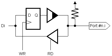
After checking the firmware, I found that, in Morphy USB-IO, a pin can be considered to have a circuit roughly equivalent to a schematics specified in the following figure.
The point is, an output buffer is not three-state controlled but is a combination of open collector (open drain) and a pull-up register. There is no explicit way to select input or output. Instead, when viewed as an output, a pin always output a value stored in the corresponding register, and, when viewed as an input, the firmware sees the wired-and of the external signal and the internal output register. That is, when a pin is to operate as an input, the corresponding output register must be set to a one (HIGH level), since the value actually read will be masked otherwise.
You can use the Morphy USB-IO I/O pins as follows:
Note that, since each pin is internally pulled-up, you cannot put an I/O pin into high impedance (Z) in Morphy USB-IO, although the CY7C63001A chip itself has the feature. This limitation comes from the firmware.
Pins on Port #0 and Port #1 have different maximum drive current. Port #0 is for small load and each pin on it can only sink up to 1.5mA at low level output. Port #1 is for heavy load and each pin can sink up to 8mA even in worst case. Leak current at high level output on both ports are limited to those supplied by the internal pull-up registers, so large current is unavailable. If you want to drive LEDs, for example, you should use pins on Port #1 in active-low.
Note that the internal pull-up registers on both ports are specified as between 8kΩ and 24kΩ.
There are two versions of Morphy USB-IO firmware. They are ver. 1 and ver. 2. Ver. 2 is latest, as far as I know.
Note that firmware version is independent from PCB versions. In particular, the PCB currently under distribution is marked as ver. 4.
The host PC recognizes Morphy USB-IO as a low speed USB device of HID class. It doesn't, however, belong to any particular HID device type, so operating systems will report it as something like "other" HID device. For example, Windows 98 reports it as "HID compatible device."
Morphy USB-IO consists of, in USB's sayings, one configuration, one interface, and two endpoints. The endpoints are: endpoint 0 to form the default control pipe and endpoint 1 to form an interrupt pipe that is mandatory in HID device specification.
Morphy USB-IO accepts the following requests through the default control pipe.
Morphy USB-IO supports the following descriptors:
Morphy USB-IO is an HID device. However, it behaves somewhat differently than usual HID devices.
To communicate with Morphy USB-IO, host PC uses two types of communication units: command and response. A command is an 8 byte data sent from the host PC to the USB-IO, which is passed as a payload of a SET REPORT request. A response is an 8 byte data sent from the USB-IO to the host PC, which is passed on an Interrupt transfer.
There is no requirement to use a command and a response as a pair. That is, the host PC may send two or more commands without receiving responses, and it may receive two or more responses without sending commands.
A command always consists of 8 bytes. The first byte of a command represents a command code that specifies the type of the command. Other 7 bytes are used for parameters to the command. When the parameters are less than 7 bytes in length, remaining bytes are unused and may be set to any value (don't care.)
Morphy USB-IO doesn't allow any command that is less than 7 bytes in length.
USB-IO version 2 firmware accepts following command codes. (The name of commands are assigned by the author of this page.)
WRITE PORT 0WRITE PORT 1READ PORT 0WRITE PORT 0 command) before issuing this command.READ PORT 1WRITE PORT 0 command) before issuing this command.WRITE PORT 0 WITH STROBE ON P1.0WRITE PORT 0. This command is only available on Morphy USB-IO ver. 2 firmware. Ver. 1 firmware doesn't support it.WRITE PORT 0 WITH STROBE ON P1.1WRITE PORT 0 WITH STROBE ON P1.0 except that the strobe signal is generated on bit 1.WRITE PORT 0 WITH STROBE ON P1.2WRITE PORT 0 WITH STROBE ON P1.0 except that the strobe signal is generated on bit 2.WRITE PORT 0 WITH STROBE ON P1.3WRITE PORT 0 WITH STROBE ON P1.0 except that the strobe signal is generated on bit 3.READ PORT 0 WITH STROBE ON P1.0READ PORT 0. This command is only available on Morphy USB-IO ver. 2 firmware. Ver. 1 firmware doesn't support it.READ PORT 0 WITH STROBE ON P1.1READ PORT 0 WITH STROBE ON P1.0 except that the strobe signal is generated on bit 1.READ PORT 0 WITH STROBE ON P1.2READ PORT 0 WITH STROBE ON P1.0 except that the strobe signal is generated on bit 2.READ PORT 0 WITH STROBE ON P1.3READ PORT 0 WITH STROBE ON P1.0 except that the strobe signal is generated on bit 3.There are two patterns of responses.
After executing a READ-type command (0x03, 0x04, 0x14, 0x15, 0x16 or 0x17), a response holds the value read from the port in its first byte (lower 4 bits of the first byte if the last command was READ PORT 1, entire 8 bits otherwise,) and the remaining seven bytes are copied from the corresponding bytes of the command. After executing a WRITE-type command (0x01, 0x02, 0x10, 0x11, 0x12 or 0x13), entire eight bytes in a response holds exact copy of the command.
Note that, Morphy USB-IO doesn't explicitly provide a way to match a response with the corresponding command. This may be a problem, although I'm not exactly sure why.
Morphy USB-IO firmware ver. 2 or later provides I/O with strobe commands (0x10 to 0x17.) In USB-IO, strobe signal is always active-low.
Strobe signal works roughly as follows:
The following issues should be noted when using strobe: